Let me add more details to better explain the task we’re trying to solve.
Environment (system configuration):
host OS: Linux;
LimeSDR library: v20.07.2 (latest);
board: LimeSDR USB (LMS7002M);
gateway: 1.4 r2.23 (latest);
work mode: pulse Tx with a low duty cycle;
utilized Rx channels: 2;
utilized Tx channels: 1 (one channel is unused).
Problem:
We’re looking for a way to send DC signal from LimeSDR board to the equepment. The DC signal has to “cover” the RF TX signal with some timings. More formal:
the output TX signal starts at Trfb moment of time and finishes at Trfe moment and has a duration Trf;
the desired DC signal should starts at Tdcb moment of time and finishes at Tdce moment and has a duration Tdc;
As I wrote, we tried to use an already implemented GPIO Tx activity indication feature, but unfortunately it doesn’t feet reguirements 3 and 4 (the GPIO signal is too short and it starts too eary actual Tdce < desired Tdcb).
Now we are looking for other possible solutions or workarounds (obviously the most preferable solutions that can be implemented with minimal SW/HW LimeSDR changes).
Ideas:
Since the second Tx channel is unused we can generate a dummy signal with desired timings as a trigger for the GPIO DC signal. But GPIO generate a DC signal based on both Tx channgels state and as result GPIO generates two signals (one desired based on the dummy Tx and another undesired based on the utilized Tx). So the question: is it possible to use only one Tx channel for Tx activity indication and ignore another?
Another possible solution is reducing of the Tdelay. In such case the undesired GPIO signal will match with the desired one and will be “covered” by them. So the question: is it possible to reduce a latency for the generated GPIO DC signal (for now the dealy is about 100 us)?
If the ideas above can’t be implemented, we think that it would be possible to use only one Tx channel and regenerate the DC signal using other GPIO ports. More detailed:
generated a RF signal from the utilized Tx channel;
use the Tx activity indication and generate DC signal from GPIO 0;
route the DC signal from the GPIO 0 on other GPIO port (let say GPIO 1);
delay and expand the DC signal;
regenerate the DC signal with the desired timings from the another GPIO port (let say GPIO 2).
Could you let us know your comments regarding this idea? Is it possible to implement with HW gateway changes? If yes, how would you estimate it’s difficulty?
So far we don’t have other ideas and If we don’t find any solution we will be forced to add one more external device that will extract an envelope from the dummy RF signal from the unused Tx channel. But in our opinion this is a worst option.
Not sure if I understand correctly. But GPIO Tx activity signal is active as long as there are data to transmit (in FPGA). So, if your second picture describes how it is working now, it is not true.
you can control signal start and end values using 0x0010 and 0x0011 FPGA registers:
0x0010[15:0] - Tx signal activity start delay value;
0x0011[15:0] - Tx signal activity end delay value.
One idea to how to advance GPIO Tx activity is to insert dummy data (zeroes) in the baseband signal. Then it will actuate GPIO in advance of your real data. Using this approach and 0x0010 and 0x0011 FPGA registers you should be able to achieve what you need I think.
Thank you for your reply and for the provided information!
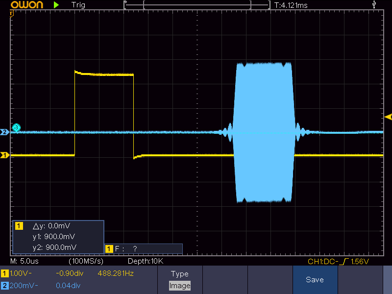
Sorry for being not correct. I wrote the diagram by memory and specified not correct timings. Please see below the correct timings that I captured using an external oscilloscope with the following board settings:
According to the diagram above the actual delay of a GPIO signal is about 30us (or 30 samples), but not 100us as I wrote. Also, it can be observed that GPIO and Tx signals have the same (or almost the same) durations.
Regarding the provided information.
This is exactly the settings that we are looking for! Together with the trick you suggested (dummy data inserting) it allows generating a GPIO signal with the desired timings! Thank you very much for your support!
We’ve spent some time to figure out how to manage by GPIO timings using the registers and eventually we come to the following conclusion:
The duration of a GPIO signal is greater or equal to the Tx signal duration, and follows to the rule:
  G = ((T + 3) / 4) * 4
  G - GPIO signal duration;
  T - Tx signal duration.
Below a table with Tx and GPIO duration relationship examples:
GPIO start can be delayed using the 0x0010[15:0] register. The LSB of the register is half of one sample (half of the current HW clock duration). The max allowed value is limited by the Tx signal duration and follows to the rule:
 G = (T - 1) * 2
 G - GPIO signal start delay;
 T - Tx signal duration.
If a written value is greater than the max allowed one the GPIO signal won’t be generated.
The maximal delay value can be increased by appending zero samples in the Tx stream as was suggested by @Zack .
GPIO finish can be delayed using the 0x0011[15:0] register. The LSB of the register is half of one sample (half of the current HW clock duration). An alternative way to manage by GPIO finish is appending zero samples in the Tx stream.
During a session (after a stream is started and before it is stopped) the GPIO start delay has the same value (no jitter is observed).
It seems that GPIO start may slightly change its position from session to session (every time when a stream is started). See diagrams below that were captured with the same board settings:
We collected data from fifty measurements and it seems that the GPIO signal start has a random delay from session to session which can take a value from the range [-half of a sample; +half of a sample].
Could you confirm that a random shift of a GPIO start is expected behavior?