
Hi,
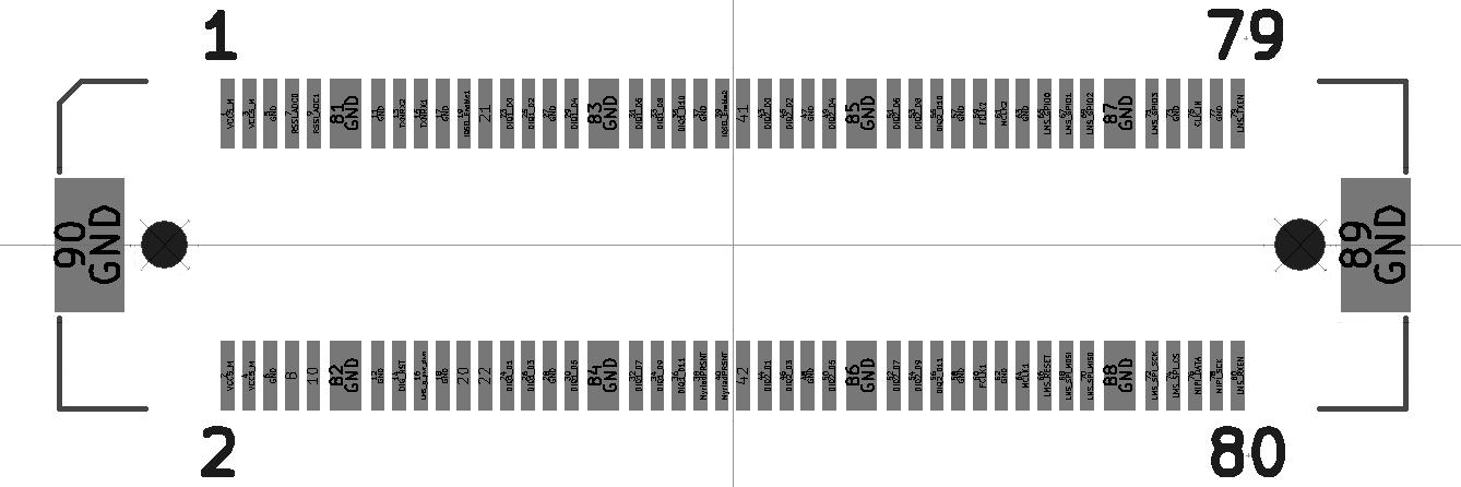
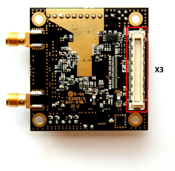
It appears there is an error in the RFDIO documentation (https://wiki.myriadrf.org/RFDIO). The black and white picture shows the digital connector (FX10B-80P/8-SV1(71)) with the chamfer near pin 1 in the upper left corner of the picture. However, in order to achieve the configuration shown for the reference development kit, the odd pins and even pins should switch places. The chamfer pin and pin 1 should be on the bottom left. This is shown in the actual PCB implementation in Zipper Development documentation. The two conflicting images are shown below. Can someone confirm the black and white footprint drawing has an error? It would also be helpful to correct this for other users and future projects.
Thanks,
Rob