LimeSDR applying reference clock

I want to provide an external clock for synchronization. From this post about the external clock specifications, @Zach says that the external clock can be 20MHz to 300MHz using the ADF4002 component. I’m trying to supply an input clock frequency of 200MHz to the J19 ref clock in port. In LimeSuite GUI, I configured the ADF4002 by making ‘Fref’ 200MHz and then click ‘Calculate R,N & Upload’:

After this, I turned on my clock signal. I also sent the signal to an oscilloscope as well as my LimeSDR. The signal looks clean and at a steady 200MHz:


The peak to peak voltage is also around 100mV so it should not be overloading the Lime.
However, when I look at my LimeSDR, the LED7 is red, meaning that the internal clock is not locked to the external clock. Here is a picture of that:

The top left light here is blinking red and green and the top right light stays red.
Any ideas on where the issue is coming from? Am I not using a steady enough clock source? Right now it is supplied by the TX port of a USRP B200mini.

Thank you.

You linked to a post that says that the REF CLK IN should be 0v (low) to 2.5v (high), not said as clear as it could have been, and then you supply it with a 100mV peak to peak relative to ground (I’m guessing).

If you read the datasheet for the ADF4002 (Phase Detector/Frequency Synthesizer), which is being used as a Phase Detector:

The absolute maximum rating for REFIN, RFINA, RFINB to GND is −0.3 V (low) to VDD + 0.3 V(high),(since VDD on the LimeSDR-USB is 3.3V, that would be between -0.3V to 3.6V maximum, exceeding that will permanently damage the ADF4002).

Under the SPECIFICATIONS section of the datasheet, REFIN has an Input Sensitivity of 0.8 V peak-to-peak minimum to 3.3 V peak-to-peak maximum, biased at 1.65 V. (The datasheet actually has “0.8 to VDD V p-p, Biased at AVDD/2”, but I substituted in 3.3V from the LimeSDR-USB schematic).

You should look at the schematic (ref: LimeSDR-USB_1v4s_schematic_r7.pdf) for the Phase detector circuit used in the LimeSDR-USB. I would be using a clock that outputs 3.3 V CMOS Logic Levels for REF CLK IN. A sine or square wave, is fine (square is better) but only if it NEVER drops below -0.3 V relative to ground, and has a minimum peak to peak voltage of at least 0.8 V. This is not something that is typically output from a SDR (not without additional circuitry, or an onboard CLK OUT).

1 Like

Thanks for the reply! That makes a lot of sense. I’m also testing the output clock (J18) from the LimeSDR and this is what I’m getting on my oscilloscope:

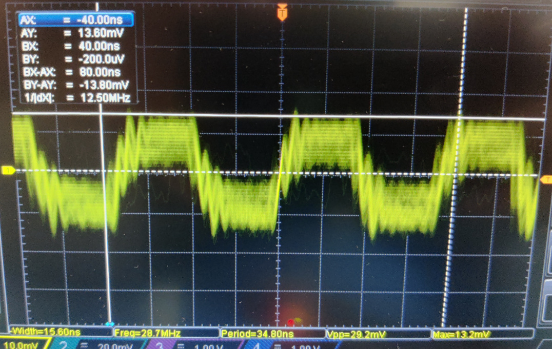
If you look in the bottom right (sorry for the bad quality) oscilloscope reads Vpp = about 30mV and max hovers around 15mV. I looked at the clock schematic and saw that the XO (Rakon E6245LF) goes into the clock buffer (LMK00105) after a few resistors and capacitors. This component outputs directly to Clk out J18 after R151 which is labeled NF. Does this stand for non-functional? If so, do I need to solder this connection to enable the external clock output? I can see on my Limesdr PCB that this is not currently soldered.
I will definitely look more closely at the documentation in the future to prevent from something bad happening!

From: https://wiki.myriadrf.org/LimeSDR-USB_hardware_description
“J18 U.FL connector Reference clock output”

You might find more information, by searching for “J18” or “R151” in this forum. NF stands for “no fit by default”. I was going to suggest searching the wiki, but there is no mention of “R151” on the wiki.

Yep, that worked. I soldered R151 on and the clock signal looks much better:

Thanks for your help. I wonder why this isn’t on by default.

1 Like

The answer was at the bottom of the thread that I linked to:

1 Like