Hello All,
I’d like to modify the LimeSDR-USB’s gateware by putting an interpolation filter along its transmit path. I’ve used Matlab to generate an interpolation filter, so that’s prepared, and I just need to figure out how to interface it with what’s already in the gateware design. I’ve taken a good look through the gateware in Quartus both in the VHD files and through the RTL Viewer and my guess would be that the easiest place to put it would be after the txiqmux block in the rxtx_top block, as seen from the gateware description document. I need a bit of help understanding exactly how the gateware works, however.
For starters, I noticed the bits leaving the txiqmux leave as 13 bit high and low lines, which become a 12 bit IQ line with a select before going to the LMS IC. According to the Stream Protocol document (https://wiki.myriadrf.org/Stream_Protocol), the 12 bit compressed samples represent a 12-bit (x2) IQ sample pair every three byte indices or basically every three times the TX_DIQ line updates. Am I getting that right? So if that is the case, in order to run the samples through the filter, I’d additionally need code to return it to a “standard” form, and then more code to convert the output of the filter back into this form.
Secondly, how should I handle the update in rate after the interpolation filter? My guess would just be to set the sample rate to the final target rate in the GNURadio design I’m testing with, but again, I’m not really sure.
Odds are I’m going about this in a silly way and there’s probably a better way to insert a filter into the FPGA. If anyone here can help me understand how to best go about this and what I should consider while doing so, I’d greatly appreciate it.
Thanks,
K
Hello lkev747,
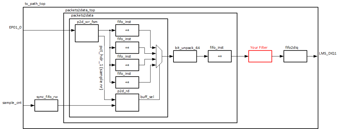
I suggest inserting your filter in tx_path_top module between packets2data_top and fifo2diq instances. This way you avoid dealing with LMS7002 interface because this is already done in fifo2diq module. Your task would be as simple as reading samples from FIFO inside packets2data_top module and writing to your created FIFO which should be connected to fifo2diq module.
See my modified tx_path_top block diagram from gateware description document.
Thanks for your replies!
@VytautasB your suggested placement of the filter seems very reasonable. From what I can glean from looking at the HDL code in the fifo2diq block, the IQ data comes in through a 48-bit wide input which I presume to contain four 12-bit numbers, or two IQ samples. Given that the data is in this format, it would make a lot of sense to place the filter there to avoid converting back and forth between the LMS7002 interface data style. However, just to confirm, the 48 bit line contains two samples, in the order I-Q-I-Q, is that correct?
There’s also the concern of whether or not inserting a filter at this position will affect the timing of the overall design. The filter will create a delay that wasn’t there before, and I fear that this may entirely break the design. Would it be right to just insert delays equal to the length of the filter to specific inputs in the fifo2diq block? Or would it be reasonable to implement the filter within the fifo2diq block itself, right after where the block reads from the 48-bit data line?
There’s also still the concern of how to address the sample rate change after applying the interpolation filter. Once again, thank you in advance for any insights you can offer!
Regards,
K
48bit bus contains two IQ samples. In SISO mode both samples are for one channel. In MIMO mode one IQ sample is for channel A and second - for channel B. See comments in tx_path_top.vhd file
As I suggested your new module (marked in red in my diagram) should contain structure something like:
- FIFO read logic which ensures that you do not read from empty FIFO in packets2data_top module
- Your interpolation filter
- FIFO write logic, which ensures that you do not write samples from interpolation filter to full FIFO.
- Aditional FIFO buffer (FIFO read ports should be connected to fifo2diq module)
This way packets2data_top and fifo2diq modules can be leaved as they are as long as you take care of both FIFO.
Regarding sample rate change you have to set TX sample rate in software to your final target after interpolation.
Hey,
So another question or two regarding this same project, specifically regarding timing considerations. Would I be wrong to assume that at the above point in the design, where the fifo_inst block outputs the 48-bit IQ data to the next block, that the data rate at this line would be half of the pre-interpolation sample rate, since each time the line updates there are 2 samples? I’m a little confused about how to handle clock inputs for a custom block, or if I should use the clock that the other blocks are all using.
Much of this confusion stems from the fields that Simulink requires when trying to model what it is that I’m trying to make. On that same note, for the 12 bits that represent the I and Q samples, should I represent them as a fixed point data type that is signed, 12 bits, with 10 fractional bits?
I probably should have realized sooner that the gateware itself perhaps isn’t the best place to necessarily implement a rate change of any sort since I don’t have an understanding of how the different blocks in the gateware design respond to the clock, and thus I couldn’t figure out how to handle the clock in the design I was building. I’ve resolved to achieve the same thing in this way:
- Set the final sample rate in the sink in the GNURadio design.
- Use an upsampler on the signal entering the sink, basically zero stuffing the signal such that the sample rate of the signal entering the sink matches the final desired sample rate.
- Implement a filter in the specified location that would calculate the proper values to the zeros, effectively achieving the desired interpolation in the output to the LMS transceiver.
This should allow me to avoid having to handle a rate transition within the gateware design, while also helping me avoid the resource consumption of implementing a filter within the software design.
And so my next question would be this: how do blocks within the TX path in the gateware design actually handle the clock and how are the clock lines set TX path with respect to the desired sample rate specified in software? I’ve read through the gateware documentation’s clock network and PLL section, but I can only assume that the pll_top module sets the LMS_FCLK1 output to the transceiver to double the desired sampling rate (on the basis that the LMS_DIQ1 output to the transceiver is 12 bits, wide enough for only an I or Q sample), and that the data rate after the fifo_inst in the packets2data module and before the fifo2diq module as mentioned above by @VytautasB is at… half the desired sampling rate (since the FIFO outputs two full I and Q samples at a time).
A good place to start would simply be how and to what the pll_top block sets the txpll_c1 and txpll_c0 lines w/r/t the LMS_MCLK1 input and the sampling rate as set by software, but I am curious about how data rates change across the TX path, if at all.
Lets say we have set 5MS/s sample rate in softwre:
LMS7002 chip provides 10MHz clock signal on LMS_MCLK1 line.
PLL inside FPGA is configured from software to output same 10MHz on txpll_c0 and txpll_c1 outputs. txpll_c0 is connected to LMS_FCLK1, LMS7002 chip uses this line to latch data on LMS_DIQ1 bus. TX path outputs data on LMS_DIQ1 bus and use txpll_c1 as a launch clock. PLL only changes phase shift on txpll_c1 output to allign LMS_DIQ1 with LMS_FCLK1 clock. In gateware PLL does not change clock rate, outputs are always set to the same rate as LMS1_MCLK1.
Data on LMS_DIQ1 changes on every edge of txpll_c1 clock (DDR mode), this means that both I and Q samples are launched in one clock cycle. Check LMS7002 datasheet , LIMELIGHT DIGITAL IQ DATA INTERFACE section for more information.
FIFO does not outputs samples every clock cycle it outputs data only when fifo2diq module asserts read request signal (Every second cycle in MIMO DDR mode and every fourth cycle in SISO DDR mode).