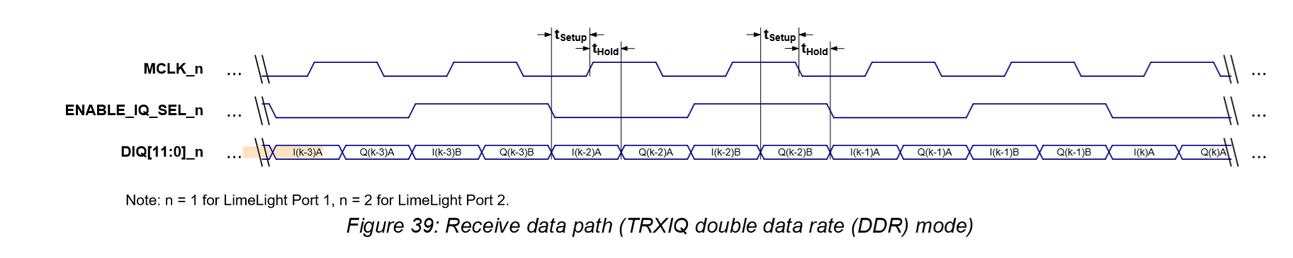
On the above timing diagramm, I understand the I-channel data and Q channel data are muxplexed.but i don’t understand the meaning of A and B here Could you pls help me to explain it? thanks very much!
Hello Ricardas,
Thanks for your quick response. According to your explanation, I am very confused. pls refer to the screemshot I posted. in the screemshot, MCLK_n, ENABLE_IQ_SEL_n and DIQ[11:0]_n, the n stands for 1 or 2, Here n should be channel number, if so, what is A and B stand for? if n , A and B all stand for n, I could not understand the meaning of the diagramm. Could you pls help me to clarify it?
There are 2 ports to the chip (the ‘n’), one is used for the RX data and other for TX.
Basically just ignore the ‘n’ and interpret ‘A’ and ‘B’ as channel numbers.
Here is example:
If ‘ENABLE_IQ_SEL’ is low -> you will receive 2 samples(I and Q) from channel A
If ‘ENABLE_IQ_SEL’ is high -> you will receive 2 samples(I and Q) from channel B